Sapphire Solutions

Single-crystal sapphire (Al203) is a hard, transparent solid material that occurs naturally and also produced, or grown, synthetically. It has high thermal conductivity, enjoys high strength, hardness and temperature resistance, has broad spectral transmission and excellent dielectric performance. Sapphire’s properties make it the ideal choice for components in harsh, destructive or biological environments.

Synthetic sapphire is produced by few active crystal growers around the world. Various growth methods produce different shapes, sizes and quality grades; raw sapphire is then fabricated through multiple process steps into finished parts.  

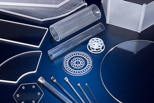
Since 2003, S & D Materials has been a trusted source for standard and custom sapphire components - sapphire windows, sapphire tubes, sapphire lenses, sapphire rods, sapphire substrates, sapphire wafers, sapphire crystal material - for OEMs, corporate and institutional end users, and a global network of trading partners serving the optical, semiconductor, defense, medical, consumer electronics and other industries. 

Sapphire

Features & Benefits

  • Features & Benefits
    • Hard & durable – Hardness, strength, resistance best among all optical materials.
    • Wide spectral range – Transmits from 0.20 µm through VIS to 3.5 µm, for use in IR optical systems, operating in the NIR and MW spectral regions.
    • Rhombohedral crystal structure – Highly anisotropic, so optical and mechanical properties vary with the crystal orientation.
    • Ideal for optics in harsh environments – Performs in high heat, extreme pressure, exposed to harmful chemicals and gases, other harsh conditions with damaging and destructive forces.
    • Many crystal growth methods – Material produced by different growth technologies can have different attributes making one type better suited for certain applications than another.
  • Why S & D Materials
    • Experienced, proven US Based supplier – Over 15 years providing sapphire products and solutions to a global customer base in multiple industries and markets.
    • Known and trusted throughout the world –The S & D brand means quality, reliability & partnership to equipment makers, technology creators, corporate and institutional end-users across every region.
    • Knowledgeable, experienced, thorough – Experience-based expertise with deep understanding of growth and fabrication processes ensure successful designs.
    • Effective, responsive communication -  We keep you updated on your quote, order, project or issue every step of the way.  ‘Same day / Next day’ response to RFQs.
    • Fast delivery – Thousands of finished parts in stock reduce lead times from months to days.
    • Managing overseas sources – Trusted, reliable liaison between a global customer base of OEMs, end users and trading partners, and the low-priced, high-quality sapphire available today in the US, Russia and the Far East.  
    • Everything fully warrantied – Sapphire products supplied by S & D Materials is fully warrantied.​

Specifications & Data

EFG
(Edge-defined, Film-fed Growth)
KYROPOLOUS
(KY)
HEM
(Heat Exchanger Method)
FEATURE / ATTRIBUTE HDSM
(Bagdasarov)
VERNEUIL
(Flame fusion)
CZOCHRALSKI
(CZ)
Melt pulled through shape-specific die - sheet (ribbon), tube or rod Top down, turn boule, fixed crucible, A axis Bottom up, fixed furnace and crucible, A axis GROWTH PROCESS Melt pulled through hot zones horizontally Sintering, pile of sapphire Pull crystal from melt and turn; diameter determined by pull rate
Alumina oxide powder Alumina oxide powder, densified pellets Crackle FEED MATERIAL Multiple types Compacted feedstock Densified Charge
Near net' shape - ribbon (sheet), tube, rod Boule (ingot) 'oversized paint can' Boule (ingot) OUTPUT SHAPE Slab Long narrow ingot (boule) Long narrow ingot (boule)
Tubes / Rods up to 30" (750+mm) long; Sheets up to 18" dia x .400" thick 13-15" dia A plane; 12" C plane; tubes 8" long 13-15" dia A plane; 12" C plane; tubes 8" long DIMENSIONS 350 x 500 x 40 mm, any orientation 13 mm dia x 50 mm length max 150 mm dia x 250 mm length
Low optical grade , structural / mechanical Excellent, good clarity, consistent high optical quality Excellent, pink tint w/o annealing Grade 1-4 OVERALL MATERIAL QUALITY Excellent, good clarity, consistent high optical quality Excellent, good clarity, consistent high optical quality Excellent, good clarity, consistent high optical quality
High Low Low DEFECT DENSITY Medium Low Low
Low Med/High High TRANSMISSION Medium High High
Average Excellent Excellent EASE OF FABRICATION Good Difficult Average
Good for high volumes; ability to grow long tube, & rod; large sheet; low pricing Excellent for optical applications; adequate for substrate material Superior optical quality, transmission through entire spectrum; low cost ADVANTAGES Crystal dimensions not possible by any other growth methods; visual seed monitoring High optical transmission, material consistency Superior optical quality, transmission through entire spectrum; low cost
Poor optical quality, high defect density Costly to abricate, cannot produce tubes Costly to abricate, cannot produce tubes DISADVANTAGES Some geometries costly to fabricate Small parts only Small parts only
Low Medium High PRICE LEVEL Medium Medium / High High

NOTE: This is not a comprehensive list of every single crystal growth technology; there are some niche-growth operations, and others that are promising but still in development. S & D will update this list as other crystal growth technologies emerge. Follow us on Twitter @sanddmaterials to receive updates.

Group Property / Attribute Value
General Chemical Formula Al2O3
Crystal Shape, Class Trigonal, hexagonal-scalenohedral
Sapphire's crystal structure is the source of its extreme strength, hardness and optical properties. When aligned, monocrystallinity is achieved with four (4) planes: C, A, M & R
Physical / Mechanical Density 3.97 gm/cm3
Shear Modulus (Modulus of Rigidity) 175 GPa (26 x 106 psi)
Flexural Strength 1035 MPa (150kpsi) parallel to C-axis (25°C)
760 MPa (110kpsi) perpendicular to C-axis (25°C)
Hardness 9 on MOHS scale (Diamond is 10)
With strength and stiffness 6 times higher than quartz, combined with excellent wear and scratch resistance, sapphire becomes the high performance choice.
Thermal Usable Temperature 2000 C
Thermal Conductivity 0.4 watts/cm °K (25°C)
0.1 watts/cm °K (1000°C)
Coefficient of Thermal Expansion (25 - 1000 C) 8.8 x 10⁻⁶ parallel to C-axis
7.9 x 10⁻⁶ perpendicular to C-axis
Sapphire's high melting point and thermal conductivity make it ideal for substrates and wafers for epitaxial growth.
Electrical Dielectric Strength 480,000 Volts/cm (1200v/mil)
Dielectric Constant 11.5 (103 - 109 Hz, 25°C) parallel to C-axis
9.3 (103 - 109 Hz, 25°C) perpendicular to C-axis
Sapphire provides a high, stable dielectric constant with the electrical insulation required for electronic substrates, RF and microwave transmitting windows and tubes.
Optical Transmittance Range 200 µm to 3500 nm
Transmission Level 80%
Birefringence 0.008 (No-Ne); eliminated along C ('optical') axis
With transmission from 200 to over 3500 nm, sapphire is used in applications requiring from UV though VIS to short wave IR (SWIR).

To see full specifications, click here

Design Tips for Sapphire Part Design

  • Material Grade - Crystal quality is defined by defect density, transmittance, clarity, elemental purity, and quantified by many factors: bubble size and density, inclusions, grain boundaries, homogeneity and color.  Material quality can vary between crystal growth methods, individual growth operations, specific furnaces, and even within a single ingot or ‘boule’ of raw material. 
  • Crystal Orientation – Sapphire crystals have several axes (C, A, R, & M) resulting in anisotropy, where optical and mechanical properties vary along different orientations.  Specifications should call out a specific crystal axis or plane
  • Birefringence is virtually eliminated along the C axis of the crystal, so for many optical applications, C axis sapphire is specified to avoid this effect.  
  • Surface Finish – Sapphire’s extreme hardness makes processing a major cost factor in the finished part. If optical transparency is not required for the application, polishing is a costly step that can be eliminated. 
  • Annealing – ‘Baking’ grown crystal in high heat (>1500˚C) for an extended time period removes stresses in the material, and any discoloration that occurs in the growth process.   Post-production annealing is often required to remove stresses from fabrication process steps 

When producing parts from sapphire, costs should be minimized and controlled by examining all aspects of the process from crystal growth through to finished part, and by determining the optimal balance between performance and production costs.

Applications and Industries

Sapphire Product Applications / Uses Industry / Markets
Sapphire Round Window Optical / UV / IR window
Sensor window
Chamber viewport
Laser window
Optical filter
Semiconductor Mfg, Optics, Defense / Aerospace, Medical, Electronics
Sapphire Square / Rectangle Window Chamber viewport
Cover screen
Waveguide, waveplate
AR / VR headsets
Insulator, protection
Defense / Aerospace, Power & Energy, Semiconductor Mfg, Consumer Technology
Sapphire Wafer Epitaxial substrate
Embedded device
Energy storage
Electronics, Power & Energy, Technology, Medical, Defense
Sapphire ring, collar, plate Insulator, protection
Semi Mfg Chamber Components
Heat Sink
High Energy Capacitor
Semiconductor Mfg., Defense, Aerospace
Sapphire Tube MW Plasma Etching
Spectroscopy
Laser / illumination systems
Semiconductor Mfg, Optics, Defense / Aerospace, Medical, Electronics
Sapphire Rod / Pin Guide Pin, Lift Pin for wafer mfg
Semi Mfg. Chamber Component
Industrial component
Semiconductor Mfg, Electronics
Sapphire Dome Missle cone
Camera dome
Button, lens
Protective window cover
Defense / Aerospace, Power & Energy, Consumer Technology
Sapphire Ingot / Core Optical Media
Raw Material
Research & Higher Ed.; Optics & Photonics
Complex geometries, features Showerhead, wafer carrier, boat
Prism, beamsplitter
Dental bracket
Laser / illumination systems
Semiconductor Mfg, Optics, Defense / Aerospace, Medical, Electronics

Contact Info

S&D Materials, LLC.
39 South Main Street Suite 222
Rochester, NH, 03867 USA

Sending an RFP?

We can help you make an RFP quick and easy. 

Download our guideline

Request A Call Back

CAPTCHA
This question is for testing whether or not you are a human visitor and to prevent automated spam submissions.